

SYKJ8810_SOT-23-6L_N_耐压20V_电流7.0A_VGS±10V
-


SYKJ8810
« Super Low Gate Charge
« Excellent Cdv/dt effect decline
« Advanced high cell density Trench technology
Product Summary
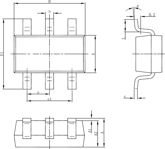
SOT23-6L
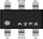
Pin Configuration
D1
D2
G1
G2
S1
S2
Absolute Maximum Ratings (TA=25℃unless otherwise noted)
Thermal Characteristic
SYKJ8810_EN_V01
第 1/7页
深圳市双宜科技有限公司
Thermal Resistance,Junction-to-Ambient (Note 2)
RθJA
100
℃/W
Parameter
Symbol
Limit
Unit
Drain-Source Voltage
VDS
20
V
Gate-Source Voltage
VGS
±10
V
Drain Current-Continuous
ID
7
A
Drain Current-Pulsed (Note 1)
IDM
25
A
Maximum Power Dissipation
PD
1.25
W
Operating Junction and Storage Temperature Range
TJ,TSTG
-55 To 150
℃
PaDcekviacge eMaMrkairnkgin
g andDeOvircdeerin
g InDfeovrimceaPtaiocknage
Reel Size
Tape width
Quantity
8205A
8205A
SOT23-6L
Ø180mm
8mm
3000 units
BVDSS
RDSON
ID
20V
14.0mΩ
7A
SYKJ8810
SYKJ8810_EN_V01
第 2/7页
深圳市双宜科技有限公司
Gate-Body Leakage Current
IGSS
VGS=±12V,VDS=0V
-
-
±100
nA
On Characteristics (Note 3)
Gate Threshold Voltage
VGS(th)
VDS=VGS,ID=250μA
0.5
0.7
1.2
V
Drain-Source On-State Resistance
RDS(ON)
VGS=4.5V, ID=4.5A
-
14
20
mΩ
VGS=2.5V, ID=3.5A
-
19
25
mΩ
Forward Transconductance
gFS
VDS=5V,ID=4.5A
-
10
-
S
Dynamic Characteristics (Note4)
Input Capacitance
Clss
VDS=10V,VGS=0V, F=1.0MHz
-
900
-
PF
Output Capacitance
Coss
-
220
-
PF
Reverse Transfer Capacitance
Crss
-
100
-
PF
Switching Characteristics (Note 4)
Turn-on Delay Time
td(on)
VDD=10V,ID=1A VGS=4.5V,RGEN=6Ω
-
10
20
nS
Turn-on Rise Time
tr
-
11
25
nS
Turn-Off Delay Time
td(off)
-
35
70
nS
Turn-Off Fall Time
tf
-
30
60
nS
Total Gate Charge
Qg
VDS=10V,ID=6A, VGS=4.5V
-
12
15
nC
Gate-Source Charge
Qgs
-
2.3
-
nC
Gate-Drain Charge
Qgd
-
1
-
nC
Drain-Source Diode Characteristics
Diode Forward Voltage (Note 3)
VSD
VGS=0V,IS=1.7A
-
0.75
1.2
V
Diode Forward Current (Note 2)
IS
-
-
6.5
A
SYKJ8810
Typical Electrical and Thermal Characteristics
Vdd
ton
toff
tr
tf
td(on)
t
d(off)
Rl
Vin
Vout
90%
90%
Vgs
VOUT
INVERTED
Rgen
G
10%
10%
90%
S
VIN
50%
50%
10%
PULSE WIDTH
Figure 1:Switching Test Circuit
Figure 2:Switching Waveforms
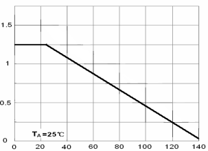
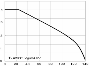
TJ-Junction Temperature(℃)
Figure 3 Power Dissipation
TJ-Junction Temperature(℃)
Figure 4 Drain Current
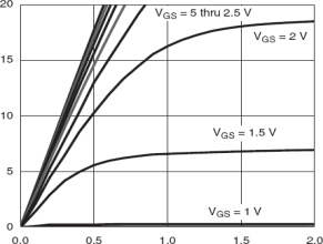
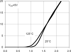
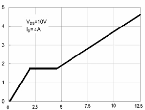
Vds Drain-Source Voltage (V)
Figure 5 Output Characteristics
ID- Drain Current (A)
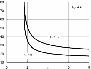
Figure 6 Drain-Source On-Resistance
SYKJ8810_EN_V01
第 3/7页
深圳市双宜科技有限公司
ID- Drain Current (A)
PD
Power(W)
Rdson On-Resistance(mΩ)
ID- Drain Current (A)
D
SYKJ8810
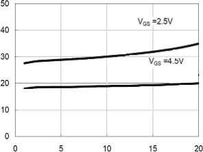
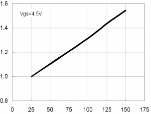
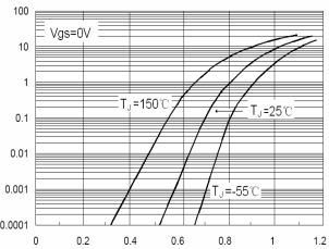
Vgs Gate-Source Voltage (V)
Figure 7 Transfer Characteristics
TJ-Junction Temperature(℃)
Figure 8 Drain-Source On-Resistance
Vgs Gate-Source Voltage (V)
Figure 9 Rdson vs Vgs
Vds Drain-Source Voltage (V)
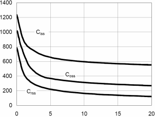
Figure 10 Capacitance vs Vds
Qg Gate Charge (nC)
Figure 11 Gate Charge
Vsd Source-Drain Voltage (V)
Figure 12 Source- Drain Diode Forward
SYKJ8810_EN_V01
第 4/7页
深圳市双宜科技有限公司
Vgs Gate-Source Voltage (V)
Rdson On-Resistance(mΩ)
ID- Drain Current (A)
Is- Reverse Drain Current (A)
C Capacitance (pF)
Normalized On-Resistance
SYKJ8810
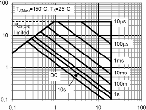
Vds Drain-Source Voltage (V)
Figure 13 Safe Operation Area
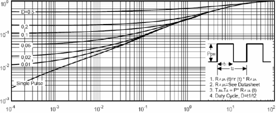
Square Wave Pluse Duration(sec)
Figure 14 Normalized Maximum Transient Thermal Impedance
SYKJ8810_EN_V01
第 5/7页
深圳市双宜科技有限公司
r(t),Normalized Effective
Transient Thermal Impedance
ID- Drain Current (A)


声明:
双宜科技保留电路及其规格书的更改权,以便为客户提供更优秀的产品,规格若有更改,恕不另行通知。
Ø
双宜科技一直致力于提高产品的质量和可靠性,然而,任何半导体产品在特定条件下都有一定
的失效或发生故障的可能,客户有责任在使用双宜产品进行产品研发时,严格按照对应规格书的要求使用双宜产品,并在进行系统设计和整机制造时遵守安全标准并采取安全措施,以避免潜在失败风险造成人身伤害或财产损失等情况。如果因为客户不当使用双宜产品而造成的人身伤害、财产损失等情况,双宜公司不承担任何责任。
Ø
本产品主要应用于消费类电子产品中,如果客户将本产品应用于医疗、军事、航天等要求极高
质量、极高可靠性的领域的产品中,其潜在失败风险所造成的人身伤害、财产损失等情况,双宜科技不承担任何责任。
Ø
本规格书所包含的信息仅作为双宜产品的应用指南,没有任何专利和知识产权的许可暗示,如
果客户侵犯了第三方的专利和知识产权,双宜科技不承担任何责任。
关于我们:
深圳市双宜科技有限公司是一家专业从事中低压场效应管、模拟集成电路芯片产品的研制、开发和销售的高新技术企业,自公司2012年成立以来,我们拥有了广大的客户群,本公司主要经营中低压场效应管,MCU设计,电源管理IC,LED驱动IC,触摸控制IC等。公司秉承坚持 " 服务第一,品质第一,客户第一 " 的原则为广大客户提供优质的服务。
客户服务中心:
深圳市双宜科技有限公司电话:0755-27863192
手机:13823527686
网址:双击打开网址了解更多详情
样片、技术支持微信:
SYKJ8810_EN_V01
第 7/7页
深圳市双宜科技有限公司
-