


SYKJ2012_SOP8_N_耐压20V_电流12.0A_VGS±12V
-


SYKJ2012
« Super Low Gate Charge
« Excellent Cdv/dt effect decline
« Advanced high cell density Trench technology
Product Summary
Description
Absolute Maximum Ratings
Thermal Data
SYKJ2012_EN_V01
第 1/6页
深圳市双宜科技有限公司
Symbol
Parameter
Max.
Unit
RθJA
Thermal Resistance Junction-ambient 1
100
℃/W
Symbol
Parameter
Rating
Units
VDS
Drain-Source Voltage
20
V
VGS
Gate-Source Voltage
±12
V
ID@TA=25℃
Continuous Drain Current, VGS @ 4.5V1
12 .0
A
ID@TA=70℃
Continuous Drain Current, VGS @ 4.5V1
7.0
A
IDM
Pulsed Drain Current2
34
A
PD@TA=25℃
Total Power Dissipation3
3
W
PD@TA=70℃
Total Power Dissipation3
0.86
W
TSTG
Storage Temperature Range
-55 to 150
℃
TJ
Operating Junction Temperature Range
-55 to 150
℃
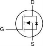
SOP8 Pin Configuration
BVDSS
RDSON
ID
20V
8mΩ
12.0A
SYKJ2012
Electrical Characteristics (TJ=25℃ unless otherwise speciied)
Notes:1. Repetitive Rating: Pulse Width Limited by Maximum Junction Temperature
2. EAS condition: TJ=25℃, VDD=10V, VG=4.5V, L=0.5mH, RG=25Ω, IAS=9.6A
3. Pulse Test: Pulse Width≤300μs, Duty Cycle≤0.5%
SYKJ2012_EN_V01
第 2/6页
深圳市双宜科技有限公司
Symbol
Parameter
Test Condition
Min.
Typ.
Max.
Units
Off Characteristic
V(BR)DSS
Drain-Source Breakdown Voltage
VGS=0V, ID=250μA
20
-
-
V
IDSS
Zero Gate Voltage Drain Current
VDS=20V, VGS=0V,
-
-
1.0
μA
IGSS
Gate to Body Leakage Current
VDS=0V, VGS=±12V
-
-
±100
nA
On Characteristics
VGS(th)
Gate Threshold Voltage
VDS=VGS, ID=250μA
0.5
0.75
1.2
V
RDS(on)
Static Drain-Source on-Resistance
note3
VGS=4.5V, ID=15A
-
8
11.2
mΩ
VGS=2.5V, ID=10A
-
11.7
17.5
Dynamic Characteristics
Ciss
Input Capacitance
VDS=10V, VGS=0V, f=1.0MHz
-
1000
-
pF
Coss
Output Capacitance
-
182
-
pF
Crss
Reverse Transfer Capacitance
-
164
-
pF
Qg
Total Gate Charge
VDS=10V, ID=15A, VGS=4.5V
-
15
-
nC
Qgs
Gate-Source Charge
-
2
-
nC
Qgd
Gate-Drain(“Miller”) Charge
-
5.2
-
nC
Switching Characteristics
td(on)
Turn-on Delay Time
VDS=10V,
ID=15A, RGEN=3Ω, VGS=4.5V
-
9
-
ns
tr
Turn-on Rise Time
-
25
-
ns
td(off)
Turn-off Delay Time
-
37
-
ns
tf
Turn-off Fall Time
-
14
-
ns
Drain-Source Diode Characteristics and Maximum Ratings
IS
Maximum Continuous Drain to Source Diode Forward Current
-
-
40
A
ISM
Maximum Pulsed Drain to Source Diode Forward Current
-
-
120
A
VSD
Drain to Source Diode Forward Voltage
VGS=0V, IS=30A
-
-
1.2
V
SYKJ2012
Typical Performance Characteristics
Figure 2: Typical Transfer Characteristics
Figure1: Output Characteristics
ID (A)
25
ID (A)
25
20
20
15
15
10
10
5
5
0
0
0
0.5
1
1.5
2
2.5
0
0.5
1
1.5
2.0
2.5
3.0
IS(A)
1E+01
21 RDS(ON) (mΩ)
1E+00
18
1E-01
15
1E-02
12
1E-03
9
1E-04
6
1E-05
0.0
0.2
0.4
0.6
0.8
1.0
0
2
4
6
8
10
12
Figure 5: Gate Charge Characteristics
VGS(V)
Figure 6: Capacitance Characteristics
C(pF)
5
4
3
2
102
1
101
0
0
3
6
9
12
15
0
4
8
12
16
20
第 3/6页
深圳市双宜科技有限公司
Ciss
Coss
Crss
VDS(V)
VDS=10V ID=4A
Qg(nC)
TJ=125℃
25℃
VSD(V)
VGS=2.5V
VGS=4.5V
ID(A)
125℃
25℃
VGS(V)
2.5V
4.5V
2.0V
VGS=1.5V
VDS(V)
SYKJ2012
Figure 7: Normalized Breakdown Voltage vs. Junction Temperature
VBR(DSS)
Figure 8: Normalized on Resistance vs. Junction Temperature
RDS(on)
2.5
1.3
1.2
2.0
1.1
1.5
1.0
1.0
0.9
0.5
0
-100
-50
0
50
100
150
200
-100
-50
0
50
100
150
200
Figure 10: Maximum Continuous Drain Current vs. Ambient Temperature
ID(A)
Figure 9: Maximum Safe Operating Area
ID(A)
10
102
8
10μs
101
100μs
6
100
1ms
4
Limited by RDS(on)
10ms
10-1
DC
TA=25℃
2
Single pulse
VDS (V)
10-2
0
0.01
0.1
1
10
0
25
50
75
100
125
150
Figure.11: Maximum Effective Transient Thermal Impedance, Junction-to-Ambient
ZthJ-A(℃/W)
103
102
101
D=0.5
D=0.2
t1
D=0.1
t2
100
D=0.05
D=0.02
D=0.01
Notes:
Single pulse
1.Duty factor D=t1/t2
2.Peak TJ=PDM*ZthJA+TA
TP(s)
10-1
10-6
10-5
10-4
10-3
10-2
10-1
100
101
SYKJ2012_EN_V01
第 4/6页
深圳市双宜科技有限公司
PDM
TA (℃)
Tj (℃)
Tj (℃)

SYKJ2012
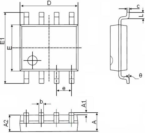
SOP-8 Package Information
SYKJ2012_EN_V01
第 5/6页
深圳市双宜科技有限公司
Symbol
Dimensions In Millimeters
Dimensions In Inches
Min.
Max.
Min.
Max.
A
1.350
1.750
0.053
0.069
A1
0.100
0.250
0.004
0.010
A2
1.350
1.550
0.053
0.061
b
0.330
0.510
0.013
0.020
c
0.170
0.250
0.006
0.010
D
4.700
5.100
0.185
0.200
E
3.800
4.000
0.150
0.157
E1
5.800
6.200
0.228
0.244
e
1.270(BSC)
0.050(BSC)
L
0.400
1.270
0.016
0.050
θ
0°
8°
0°
8°


声明:
双宜科技保留电路及其规格书的更改权,以便为客户提供更优秀的产品,规格若有更改,恕不另行通知。
Ø
双宜科技一直致力于提高产品的质量和可靠性,然而,任何半导体产品在特定条件下都有一定
的失效或发生故障的可能,客户有责任在使用双宜产品进行产品研发时,严格按照对应规格书的要求使用双宜产品,并在进行系统设计和整机制造时遵守安全标准并采取安全措施,以避免潜在失败风险造成人身伤害或财产损失等情况。如果因为客户不当使用双宜产品而造成的人身伤害、财产损失等情况,双宜公司不承担任何责任。
Ø
本产品主要应用于消费类电子产品中,如果客户将本产品应用于医疗、军事、航天等要求极高
质量、极高可靠性的领域的产品中,其潜在失败风险所造成的人身伤害、财产损失等情况,双宜科技不承担任何责任。
Ø
本规格书所包含的信息仅作为双宜产品的应用指南,没有任何专利和知识产权的许可暗示,如
果客户侵犯了第三方的专利和知识产权,双宜科技不承担任何责任。
关于我们:
深圳市双宜科技有限公司是一家专业从事中低压场效应管、模拟集成电路芯片产品的研制、开发和销售的高新技术企业,自公司2012年成立以来,我们拥有了广大的客户群,本公司主要经营中低压场效应管,MCU设计,电源管理IC,LED驱动IC,触摸控制IC等。公司秉承坚持 " 服务第一,品质第一,客户第一 " 的原则为广大客户提供优质的服务。
客户服务中心:
深圳市双宜科技有限公司电话:0755-27863192
手机:13823527686
网址:双击打开网址了解更多详情
样片、技术支持微信:
SYKJ2012_EN_V01
第 6/6页
深圳市双宜科技有限公司
-


