


SYKJ2012A_SOP8_N_耐压20V_电流10.0A_VGS±12V
-


SYKJ2012A
« 100% EAS Guaranteed
« Green Device Available
« Super Low Gate Charge
« Excellent CdV/dt effect decline
« Advanced high cell density Trench technology
The SYKJ2012A is the high cell density trenched N-ch MOSFETs, which provide excellent RDSON and gate charge for most of the synchronous buck converter applications. The SYKJ2012A meet the RoHS and Green Product requirement, 100% EAS guaranteed
with full function reliability approved.
Absolute Maximum Rating (TJ=25°C unless otherwise noted)
Thermal Characteristics
SYKJ2012A_EN_V01
第 1/6页
深圳市双宜科技有限公司
Parameter
Symbol
Value
Unit
Thermal Resistance from Junction to Ambient2
RθJA
90
°C/W
Parameter
Symbol
Value
Unit
Drain-Source Voltage
VDS
20
V
Gate-Source Voltage
VGS
±12
V
Continuous Drain Current
TA= 25°C
ID
10
A
Pulsed Drain Current1
IDM
20
A
Power Dissipation
TA= 25°C
PD
2.25
W
Operating Junction and Storage Temperature Range
TJ, TSTG
-55 to 150
°C
Description
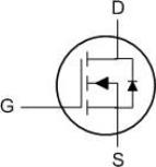
SOP8 Pin Configuration
BVDSS
RDSON
ID
20V
12mΩ
10A
Product Summary
SYKJ2012A
Electrical Characteristics (TJ=25°C unless otherwise noted)
Notes:
1. Repetitive rating, pulse width limited by junction temperature TJ(MAX)=150°C.
2. The data tested by surface mounted on a 1 inch2 FR-4 board with 2OZ copper, The value in any given application depends on the user's specific board design.
3. Pulse Test: Pulse width≤300μs, duty cycle≤2%.
4. This value is guaranteed by design hence it is not included in the production test.
SYKJ2012A_EN_V01
第 2/6页
深圳市双宜科技有限公司
Parameter
Symbol
Test Condition
Min.
Typ.
Max.
Unit
Static Characteristics
Drain-Source Breakdown Voltage
BVDSS
VGS = 0 V, ID = 250µA
20
-
-
V
Gate Leakage Current
IGSS
VGS = ±12V, VDS = 0 V
-
-
±100
nA
Drain Cut-off Current
IDSS
VDS = 20V, VGS = 0 V
-
-
1
µA
Gate Threshold Voltage
VGS(th)
VGS = VDS, ID = 250µA
0.45
0.7
1
V
Drain-Source On-State Resistance3
RDS(on)
VGS = 4.5V, ID =5A
-
12
15
mΩ
VGS = 2.5V, ID = 4.7A
-
17
21
VGS = 1.8V, ID = 4.3A
-
28
50
Dynamic Characteristics4
Input Capacitance
Ciss
VGS = 0V, VDS = 10V,
f = 1MHz
-
700
-
pF
Output Capacitance
Coss
-
120
-
Reverse Transfer Capacitance
Crss
-
105
-
Switching Characteristics4
Total Gate Charge
Qg
VGS= 4.5V, VDS= 10V, ID= 5A
-
10.5
-
nC
Gate-Source Charge
Qgs
-
2
-
Gate-Drain Charge
Qgd
-
2.5
-
Turn-On Time
td(on)
VGEN= 5V, VDD = 10V, ID = 5A,RG= 3Ω,
-
10
-
ns
Rise Time
tr
-
20
-
Turn-Off Time
td(off)
-
32
-
Fall Time
tf
-
12
-
Source-Drain Diode Characteristics
Body Diode Voltage3
VSD
IS=4A, VGS = 0V
-
-
1.2
V
Continuous Source Current
IS
-
-
30
A
SYKJ2012A
Typical Characteristics
20
20
15
15
10
10
5
5
0
0
0
1
2
3
4
5
0
0.5
1
1.5
2
2.5
Drain−source voltage VDS (V)
Gate−source voltage VGS (V)
Figure 1. Output Characteristics
Figure 2. Transfer Characteristics
10
100
8
80
6
60
4
40
2
20
0
0
0.2
0.4
0.6
0.8
1.0
1.2
0
2
4
6
8
Gate−source voltage VGS (V)
Source−drain voltage VSD (V)
Figure 4. RDS(ON) vs. VGS
Figure 3. Forward Characteristics of Reverse
50
2.0
40
1.5
30
20
1.0
10
0
0.5
0
2
4
6
-50 -25
0
25 50 75 100 125
Temperature Tj(°C)
150
Drain current ID (A)
Figure 5. RDS(ON) vs. ID
Figure 6. Normalized RDS(on) vs. Temperature
SYKJ2012A_EN_V01
第 3/6页
深圳市双宜科技有限公司
On-Resistance
RDS (on) (mΩ)
Drain current ID (A)
Source current IS (A)
Normalized RDS (on)
On-Resistance
RDS (on) (mΩ)
Drain current ID (A)
VGS = 1.8V
VGS = 2.5V
VGS = 4.5V
ID= 5A
VDS= 3V
VGS =
VGS = VGS =
4.5V
2.5V
2V
VGS = 1.5V
SYKJ2012A
SYKJ2012A_EN_V01
第 4/6页
深圳市双宜科技有限公司
Capacitance(pF)
10000
1000
100
10
1
0 5 10 15 20
Drain-source voltage VDS(V)
Figure 7. Capacitance Characteristics
Figure 8. Gate Charge Characteristics
Ciss
Coss
Crss
F=1.0MHz

SYKJ2012A
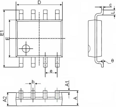
SOP-8 Package Information
SYKJ2012A_EN_V01
第 5/6页
深圳市双宜科技有限公司
Symbol
Dimensions In Millimeters
Dimensions In Inches
Min.
Max.
Min.
Max.
A
1.350
1.750
0.053
0.069
A1
0.100
0.250
0.004
0.010
A2
1.350
1.550
0.053
0.061
b
0.330
0.510
0.013
0.020
c
0.170
0.250
0.006
0.010
D
4.700
5.100
0.185
0.200
E
3.800
4.000
0.150
0.157
E1
5.800
6.200
0.228
0.244
e
1.270(BSC)
0.050(BSC)
L
0.400
1.270
0.016
0.050
θ
0°
8°
0°
8°


声明:
双宜科技保留电路及其规格书的更改权,以便为客户提供更优秀的产品,规格若有更改,恕不另行通知。
Ø
双宜科技一直致力于提高产品的质量和可靠性,然而,任何半导体产品在特定条件下都有一定
的失效或发生故障的可能,客户有责任在使用双宜产品进行产品研发时,严格按照对应规格书的要求使用双宜产品,并在进行系统设计和整机制造时遵守安全标准并采取安全措施,以避免潜在失败风险造成人身伤害或财产损失等情况。如果因为客户不当使用双宜产品而造成的人身伤害、财产损失等情况,双宜公司不承担任何责任。
Ø
本产品主要应用于消费类电子产品中,如果客户将本产品应用于医疗、军事、航天等要求极高
质量、极高可靠性的领域的产品中,其潜在失败风险所造成的人身伤害、财产损失等情况,双宜科技不承担任何责任。
Ø
本规格书所包含的信息仅作为双宜产品的应用指南,没有任何专利和知识产权的许可暗示,如
果客户侵犯了第三方的专利和知识产权,双宜科技不承担任何责任。
关于我们:
深圳市双宜科技有限公司是一家专业从事中低压场效应管、模拟集成电路芯片产品的研制、开发和销售的高新技术企业,自公司2012年成立以来,我们拥有了广大的客户群,本公司主要经营中低压场效应管,MCU设计,电源管理IC,LED驱动IC,触摸控制IC等。公司秉承坚持 " 服务第一,品质第一,客户第一 " 的原则为广大客户提供优质的服务。
客户服务中心:
深圳市双宜科技有限公司电话:0755-27863192
手机:13823527686
网址:双击打开网址了解更多详情
样片、技术支持微信:
SYKJ2012A_EN_V01
第 6/6页
深圳市双宜科技有限公司
-


